Introduction to PN Junction Diodes
PN junction diodes are pivotal components in modern electronics. They act as gatekeepers, guiding the flow of electrical current in one direction while blocking it in the opposite. These semiconductor devices are created when a p-type semiconductor, rich in positive charge carriers called ‘holes’, and an n-type semiconductor, laden with negative charge carriers or ‘electrons’, are joined together.
Basic Definition and Structure
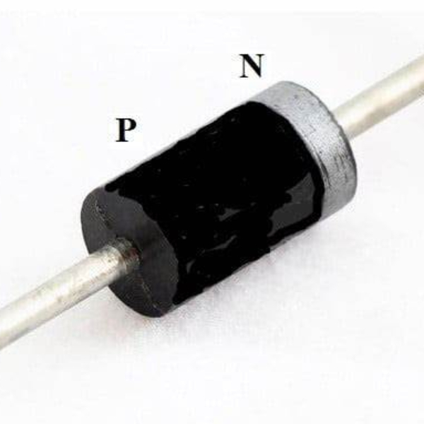
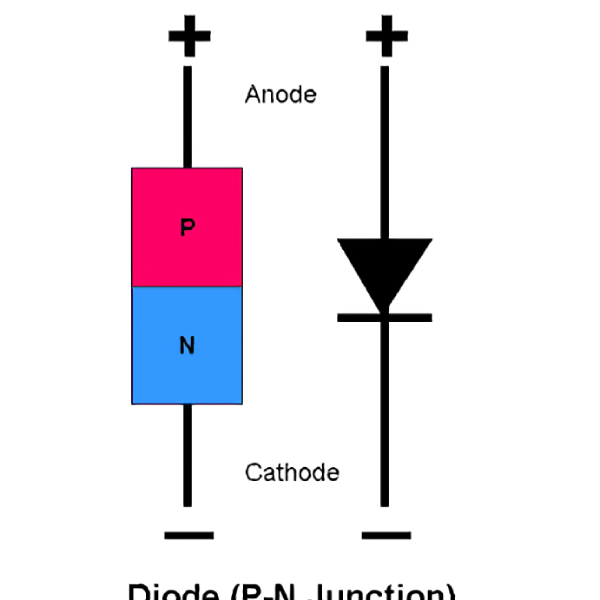
A PN junction diode consists of two contrasting types of semiconductor materials: p-type and n-type. The ‘PN’ denotes the junction point where these materials meet, which forms the core part of the diode. Here, an intricate balance of electrons and holes allows the diode to conduct and control electrical current effectively.
The Importance of PN Junction Diodes in Electronics
In electronic circuits, PN junction diodes are crucial for their versatility and functionality. They are used widely in rectifying alternating current (AC) to direct current (DC), which is essential for electronic devices to function. Additionally, they serve as voltage regulators, ensuring stable power supply within circuits. Their ability to switch currents on and off quickly makes them invaluable in digital electronics. The primary diode purpose in electronic circuits is to rectify AC to DC, regulate voltage, and enable rapid switching in digital applications.
Formation of PN Junction Diodes
The formation of PN junction diodes is a nuanced process, integral to advancing the functionality of various electronic devices.
The Doping Process
Doping transforms pure semiconductors into n-type or p-type materials, essential for diode functionality. This process involves introducing impurities into a semiconductor. For instance, adding trivalent elements like boron to silicon creates a p-type material rich in ‘holes’. Conversely, adding pentavalent elements such as phosphorus gives rise to an n-type material abundant in electrons.
Creation of the Depletion Zone
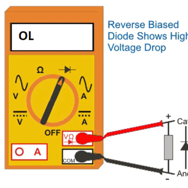
The p-type and n-type materials, when combined, form a PN junction creating a depletion zone. This zone is devoid of any free charge carriers—neither electrons nor holes. It acts as a barrier that controls the flow of electric current. The junction’s potential difference prevents charge carriers from crossing the depletion zone under normal, unbiased conditions. This characteristic is pivotal for the diode’s functioning. In a diode setting on a multimeter, the PN junction’s depletion zone allows for measuring current flow, demonstrating the diode’s essential function as a current control device.
How PN Junction Diodes Operate
The operation of PN junction diodes relies on two key processes: diffusion and drift.
Understanding Diffusion and Drift
Diffusion in PN junction diodes occurs when charge carriers move from regions of high concentration to low concentration. In these diodes, holes from the p-type material spread into the n-type material, and electrons do the opposite. Drift, on the other hand, is when charge carriers move due to the electric field in the depletion zone. This occurs in the opposite direction to diffusion. In a diode, the anode attracts electrons, while the cathode attracts holes, facilitating both diffusion and drift processes across the junction.
The Role of the Depletion Zone
The depletion zone is crucial to the diode’s functionality. It acts like a barrier to charge carrier movement when it’s not under bias. When a voltage is applied (forward or reverse bias), it either narrows or widens, controlling the current flow. In a sense, the depletion zone acts as a switch, dictating when the diode will conduct electricity.
Biasing Conditions for PN Junction Diodes
The biasing conditions of a PN junction diode are crucial for its operation. They determine how the diode behaves under different electrical environments. Let’s dive into these conditions and see how they influence diode functionality.
Zero Bias ? The Natural State
In zero bias, no external voltage is applied to the PN junction. In this state, the depletion zone remains intact, acting as a barrier that stops the flow of charge carriers. This prevents any significant current from flowing through the diode, essentially turning it off.
Forward Bias ? Allowing Flow of Current
Forward biasing occurs when the positive terminal of the power source connects to the p-type material, and the negative to the n-type. This setup reduces the width of the depletion zone. As the depletion barrier lessens, charge carriers can cross more easily. Consequently, current starts flowing through the diode. The junction diode allows more holes and electrons to combine on reaching this state, enabling electricity pass through.
Reverse Bias ? Blocking Current Flow
Reverse biasing happens when the connections are switched: the positive terminal links to the n-type and the negative to the p-type. This increases the depletion zone’s width, further blocking charge carriers. The wider the zone, the harder it is for electric current to flow, enhancing the diode’s effectiveness as an off switch. In reverse bias, the diode effectively stops current, ensuring no accidental charges slip through.
PN Junction Diode Formula
Understanding the formula that describes a PN junction diode is crucial for grasping how these semiconductors function under different conditions.
Explanation of the Formula Variables
The PN junction diode formula is given by:
egin{equation}
E_0 = V_T imes ext{ln}igg(\frac{N_D \times N_A}{n_i^2}\bigg)
\end{equation}
where:
- (E_0) represents the zero bias junction voltage,
- (V_T) is known as the thermal voltage, usually about 26mV at room temperature,
- (N_D) and (N_A) signify the concentration of donors and acceptors (impurities),
- (n_i) stands for the intrinsic carrier concentration.
This equation helps to understand how voltage changes with these variables under certain conditions.
The Impact of Temperature and Doping Levels
Temperature and doping levels significantly affect the performance of PN junction diodes. As temperature increases, the intrinsic carrier concentration ((n_i)) rises, which impacts the diode’s functionality. Increased doping levels (higher (N_D) or (N_A)) modify the junction’s properties, resulting in changes in the voltage (
((E_0))). These alterations influence both the efficiency and the operational capacity of the diode in electronic circuits. Understanding these factors is essential for optimizing diode performance in practical applications.
Applications of PN Junction Diodes
PN Junction Diodes find application in various fields due to their unique ability to control electrical current.
In Rectifiers
Rectifiers use PN junction diodes to convert alternating current (AC) to direct current (DC). This conversion is crucial for devices that operate only on DC.
In Voltage Regulation
Voltage regulators incorporate PN junction diodes to maintain a constant voltage level. These diodes help stabilize voltage fluctuations, which can harm delicate electronics.
As Switches in Circuits
In digital circuits, PN Junction Diodes act as rapid switches. They turn current flow on and off quickly, essential for processing digital signals.
VI Characteristics of PN Junction Diodes
Understanding the behavior of PN junction diodes under varying voltage and current conditions is essential. This understanding is encapsulated in what are known as the Voltage-Current (VI) characteristics.
Understanding the VI Curve
The VI curve of a PN junction diode showcases how voltage across the diode and the current through it are related to each other. This curve is a crucial graphical representation that helps to predict the behavior of the diode in different circuit conditions.
- On the curve, the x-axis represents the voltage applied to the diode.
- The y-axis corresponds to the current flowing through the diode.
- The curve helps in identifying the operational states of the diode such as the forward bias region, the reverse bias region, and the breakdown region.
Analyzing under Different Conditions
When the PN junction diode is forward-biased, it conducts electricity and the curve shows a steep increase in current as voltage is increased past a certain threshold. This threshold is typically around 0.7 volts for silicon diodes. In this state, the diode allows charge carriers to flow across the junction, resulting in the passage of current.
In reverse bias, the curve is mostly flat, indicating minimal current flow. This continues until the breakdown voltage is reached. At this critical point, a sudden increase in current occurs which can potentially damage the diode if the current is not limited.
By analyzing the VI characteristics, engineers can design circuits with diode specs that work efficiently for intended applications such as signal processing, power conversion, or as protective devices.

